Nanoscience has progressed over the last 50 years from a scattered set of basic but outstanding breakthroughs to hundreds of research groups world-wide, continuously announcing the discovery of novel nanomaterials and fascinating nanodevices. Nanotechnology is becoming real; in fact, many of these advances have become part of our daily life. This article describes the basic features characterizing current research in nanotechnology and its main application sectors. In addition, this study also covers other issues like funding or public perception of this multidisciplinary field.
The prefix nano (which comes from the Greek word meaning “small”) equals one billionth of the unit of measurement to which it is attached. Thus, a nanometre (1 nm) is a length equal to one millionth of a millimetre. Arbitrarily defined as the so-called nanoscale, lengths or sizes range between 1 nm and 100 nm. At the nanoscale we find atoms, molecules, proteins, viruses, chains of deoxyribonucleic acid (DNA), carbon nanotubes, nanoparticles… They are all nano-objects of interest within the scope of nanoscience and nano-technology.
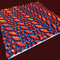
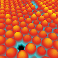
This image has been taken using Scanning Tunnelling Microscopy (STM) and shows a gold surface covered with two types of molecules of planar structure: Diindenoperylene (DIP) and Copper Phthalocyanine (CuPc). The ordered structure has been achieved using Molecular Beam Epitaxy (MBE) techniques. The molecules are arranged spontaneously (self-assembled) in alternating rows following well-defined directions. This is an example of massive bottom-up technology, which will one day allow large-scale manufacturing of devices. The author of this picture, entitled (Nano)-blossoms in the Dark, is Prof. Garcia de Oteyza, from the Max Planck Institute of Materials Research (Stuttgart, Germany). This image was one of the finalists in the SPMAGE07 international contest. / D. García de Oteyza
The term nanoscience refers to research that endeavours to understand the structure and properties of materials and objects that fall within the size range characteristic of nanoscale. Nanotechnology, works from this knowledge base to produce materials, structures and devices that provide new properties due to their nanometric size. The prefix nano is also used with existing disciplines, when we want to emphasize that the aim is to study nanoscale phenomena. Thus we speak of nanoelectronics, nanochemistry, nanophotonics, nanobiotechnology, etc.
Nanoscience and nanotechnology underwent relatively quiet development until the nineties. Almost half a century has passed since the visionary speech by R. Feynman, which led us to dream of understanding and mastering matter at the nanoscale. The very term nanotechnology has already been with us 35 years, since it was coined by N. Taniguchi in 1974. In the past two decades, the so-called proximity microscopes, invented by H. Rohrer and G. Binnig, have become common tools, used to observe and handle nano-objects. Carbon nanotubes, major players in nanoscience, were discovered in 1991 by the Japanese researcher S. Iijima. Now, as the first decade of the twentieth century draws to a close, we are aware of the long way we have come.
There has been more evident promotion of nanotechnology over the last ten years, thanks to the huge financial investment made by governments and companies in more developed countries to promote research into nanotechnology and knowledge transfer to the productive sector. There is widespread conviction that this newfound knowledge will help establish a new economic model, which may be the gateway to the much desired sustainable development. Nor should we forget another key factor: nanotechnology is expected to generate business, which could reach two billion Euros in 2015.
Top-down, bottom-up
One of the greatest problems facing nanotechnology is the difficulty of scaling up to the industrial dimension. Its incorporation to industry can be done in two ways. On the one hand there are the so-called top-down processes, which start off with larger systems to obtain (via cutting, polishing, lithography techniques, etc.) systems with nanometric parts. This approach, for example, has enabled a continual increase in the density of transistors incorporated into silicon wafers. On the other hand, nanotechnology offers another alternative, the so-called bottom-up approach, starting off with small elements (atoms, molecules, DNA chains, nanostructures…) to build complex systems able to perform a variety of functions. The only fully functioning system following the bottom-up procedure is life itself, with biological structures and operating mechanisms constituting the archetype for the design of bottom-up technologies.
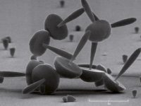
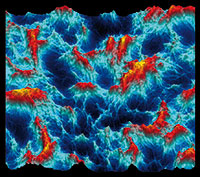
Atomic force microscopy is a powerful tool to observe and modify biological samples at nanoscale. This image shows beta-amyloidal peptide filaments, involved in Alzheimer’s disease, deposited on mica. These observations can be made in liquid media, thus opening the gateway to the study of biological processes in real time. The author of this picture, entitled Venis of Coral, is F. Mantegazza, from the University of Milan Bicocca (Italy). This image was awarded a prize in the SPMAGE09 international contest. / F. Mantegazza
Nanotechnology is a multidisciplinary field in which chemists, biologists, physicists and engineers converge. From such meeting of minds, we can hope for unprecedented approaches, likely to provide new solutions to problems raised in a large number of application sectors. Here are a few nanotechnology-based proposals for some of these sectors.
Biotecnnology and medicine
Within this ambit, new techniques are underway for observing biological phenomena with the help of equipment like atomic force microscopes. Also new diagnostic means are being implemented based on functionalized nanoparticles (i.e., coated with a material that confers new properties, for instance to detect the focus of a disease). In certain cases, these nanoparticles, which are being used as optical or magnetic markers to detect diseases early on, can also act as therapeutic agents, destroying the diseased tissue to which they adhere. The diagnosis of diseases may benefit from the development of nanoelectronic sensors that accurately monitor our health. Different nanoelectronic devices will also be used to restore visual and auditory abilities of patients suffering from loss of sight or hearing. There is also a surge of interest in research aiming to develop systems that can dispense drugs at the proper time and place. Finally, biocompatible nanomaterials are already being used to manufacture more resistant prosthesis.
Energy and environment
Without doubt, these issues have gained importance due to evidence of climate change and the related containment measures that seek to reduce carbon dioxide emissions, the need to turn to renewable energy and optimize the use of conventional energy sources. Other issues, such as providing universal access to water resources and the control and remediation of pollution, are also high priority in our search for global sustainable development. In the field of energy, nanopore and nanoparticle catalysts remain cornerstones in obtaining petrol as well as a host of other industrial chemical processes. Nanostructured materials will be applied in fuel cells, hydrogen production and the next-generation alkaline battery. Solar panels will become more efficient through the use of nanostructured materials (be they silicon-based or based on other organic or inorganic semiconductors). Wind power can gain efficiency thanks to nanocomposites, allowing larger turbines to be built. With regard to water management, nanotechnology will improve current techniques of desalination, water treatment and purification. Pollution can be detected more quickly and efficiently through the use of nanosensory networks.
Fullerenes, C60 being the best known example, are carbon-based molecules which have been proposed for use as current rectifying elements in electronic circuits of the future. This image, taken by STM microscopy, shows pairs and trimers of C60 molecules trapped in a porous structure of high thermal stability, with a honeycomb-type morphology formed by a derivative of perylene. The regular pattern of hexagonal holes provides anchorage points, where other molecules can be deposited and fixed. This image, entitled C60 Trapped within a Nano-porous Network, was taken by M. Störh, from the University of Basel (Switzerland), and was a finalist in the SPMAGE07 international contest. / M. Störh
Information and communication technologies
These technologies have been pioneer in all aspects of miniaturization, thus the density of transistors in a processor, or of the bits in a data storage system, has increased by several orders of magnitude over the last four decades. One could say that the manufacture of electronic devices entered the field of nanotechnology some ten years ago. This rate is expected to continue as long as silicon can still be used. However, when the properties of silicon can be compressed no more, alternatives will be sought to provide the same services at similar costs. Whichever alternative is adopted, we can be reasonably sure that it will be based on nanotechnological developments that are currently underway in laboratories. Among these we should highlight those based on using carbon molecules and nanotubes as building blocks for the processors and memories of the future. Nor should we forget the development of nanophotonic techniques for information processing. In these cases, nanotechnology will be used to manufacture, with nanometric precision, light-manipulating structures.
Traditional industries
Here we refer to the kind of nanotechnology that is starting to be applied in sectors such as construction, the automotive sector, the manufacture of textiles, cosmetics, etc. In this context, nanotechnology is a supplier of new materials that give an added value to products. For example, carbon nanotubes are already being used to reinforce building materials, or certain vehicle parts, or sports equipment. Various hydrophobic nanoparticles are incorporated into materials to provide dirt-proof or anti-fogging surfaces. Silver nanoparticles, with bactericidal properties, are integrated into textiles or air-conditioner filters. Paint and varnish formulations include nanoparticles to make them more resistant to small scratches. Traditional industries will benefit from nanosensors, which, incorporated to different materials, provide information on both environmental variables (temperature, humidity, etc.) and the material itself (degree of fatigue, emergence of defects, etc.). Finally, we should mention the numerous nanoporous materials that are already being used in the cosmetics industry to dispense substances. Also, this sector is using nanoparticles to block ultraviolet radiation in both makeup and sunscreen creams.
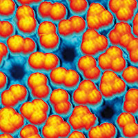
This image shows an ordered structure of polystyrene nanospheres measuring 200 nm in diameter, obtained by self-assembly from a colloidal solution. This structure forms what is called a photonic crystal, which can be used to control and manipulate light, and will be highly instrumental in the development of future optical computers. The image shows some defects in the two-dimensional crystalline structure. This image is entitled Aesthetic Imperfections, and was presented by D. Danzebrik, from the PTB institute Germany, for the SPMAGE09 international contest. / D. Danzebrik
Euphoria, fear, concern and risk control
With so many applications underway or on the horizon, we would expect juicy profits for leaders in the application of nanotechnology. However, the arrival of nano-applications is subject to the publics’ perception of nanotechnology. Over the last decade, we have gone from having a positive and hopeful vision of nanotechnology to a state of uncertainty about its possible impact. This change in perception can be put down to numerous groups and organizations that have sounded the alarm, concerned about the proliferation of nano products on the market and the lack of knowledge regarding their potential impact on the health of workers, consumers or the environment. Various forums have even proposed the suspension of nano product trade.
Such fears could lead to the withdrawal of investment in nanotechnology and delay the arrival of the much-promised industrial revolution of the twenty-first century. Governments and businesses alike have reacted relatively fast, and launched projects to study the real impact of nanotechnology on the environment, on those who work with it and end users. All these studies have given rise to a new discipline: nanoecotoxicology. Furthermore, emphasis is being placed on applying precautionary principles to minimize the possible risk in laboratories or production facilities. However, it is fairly complex to manage a risk whose magnitude and consequences are unknown. All the aspects of decision-making within this new context are leading to the study of nanoethics. Mention should also be made of the patent need to improve training and information on this topic, and accordingly many governments have taken serious steps to provide educational and informative materials, which are made available to the public in the press, museums, on television, etc.
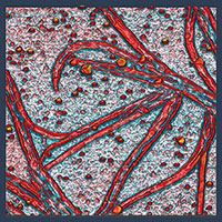
The AFM image shows the topography of hydrogel fibres grown on mica from calixarene and NaBr, in the presence of moisture. The maximum heights observed are 50 nm. Such materials have been proposed for use as chemical sensors and controlled drug-release systems. This image was taken by T. Becker, Curtin University of Technology (Perth, Australia), entitled Hydrogel Network it was a finalist in the SPMAGE09 international contest. / T. Becker
For all these reasons, it is patent that the transversal nature of nanoscience and nanotechnology reaches far beyond the purely experimental disciplines and is strongly linked to issues of job safety, environmental impact, sociological and cultural issues, ethical aspects, the emergence of new legal issues, etc.
Looking ahead
No-one can doubt the role that nanotechnology will play in our future, both medium and long term, thus it is imperative to be properly prepared to help construct this new scientific-technical paradigm and consolidate its transference to the productive sectors and society. It takes determination to continue investing in ambitious projects and to promote efficient and professionalized transfer mechanisms. Otherwise, we will continue to generate competitive nanoscience, but carry on increasing our trade deficit in technology-based products. It may be true that the current economic situation does not call for optimism, but this is precisely the moment to keep up investments in leading areas like nanoscience and nanotechnology, and to optimize on existing resources. Nor should we neglect training in nanotechnology at all educational levels, from primary to postgraduate, implementing programs similar to those existing in other countries. After all, society should be both beneficiary and accomplice in nanotechnological development.
Nanotechnology in Spain: organizational networks and initiatives
Profits from nanotechnology will be reaped by those countries that lead research in nanoscience and are able to transfer it to the productive sector. But what is the situation in Spain? Here nanotechnology has developed following a similar pattern to that of -other scientific disciplines, with their pros and cons, and currently there are about three hundred research groups covering virtually the whole range of nanoscience and nanotechnology-related topics.

Since 2000, given the global impact of the National Nanotechnology Initiative in the U.S.A. and European Union policies, Spanish researchers were organized in networks like the former Nanoscience Network or the NanoSpain network. These structures helped to put pressure on government and managed to implement the Strategic Action Plan in Nanoscience and Nanotechnology within the National Plans for Research, Development and Innovation during the periods 2004-2007 and 2008-2011. Further to these strategic initiatives, the Programa Ingenio 2010, which aims to speed up scientific and technological convergence in the European Union, has promo-ted research in nanoscience and nanotechnology through CENIT and Consolider programs. Besides these efforts, we should also mention those made by local governments in the autonomous regions. All these new planning and funding initiatives have helped to create a positive environment in the field of nanotechnology, which is reflected by the opening of almost a dozen new research centres. Overall, the investment made has improved the country’s research potential; however, it is insufficient to achieve a position of leadership internationally and, what is more, the current economic situation may curtail some of the progress made so far.
Bibliography
Azkarate, G. (dir.), 2008. Aplicaciones Industriales de las Nanotecnologías en España en el Horizonte 2020 [on line]. Fundación OPTI/Fundación INASMET-TECNALIA. Madrid. Available in: <http://www.opti.org/publicaciones/pdf/texto10.pdf>
Correia, A.; Sáenz, J. J. & P. A. Serena, 2006. «El lento despertar de la nanotecnología en España». Revista Sistema Madri+d, 15: 3.
Correia, A. (coord.), 2008. Nanociencia y nanotecnología en España: Un análisis de la situación presente y de las perspectivas de futuro [on line]. Fundación Phantoms. Madrid. Available in: <http://www.phantomsnet.net/Resources/NNE.php>
Delgado, G. C., 2008. Guerra por lo invisible: negocio, implicaciones y riesgos de la nanotecnología. Ceeich/UNAM. México.
Fontela, E. et al., 2006. «Convergencia NBIC 2005. El desafío de la Convergencia de las Nuevas Tecnologías (Nano-Bio-Info-Cogno)». Fundación Escuela de Organización Industrial (EOI). Madrid.
Martín-Gago, J. A. et al., 2008. Unidad Didáctica Nanociencia y Nanotecnología. Entre la ciencia ficción del presente y la tecnología del futuro. FECYT. Madrid.
Serena, P. A. & A. Correia, 2003. «Nanotecnología: el motor de la próxima revolución tecnológica». Apuntes de Ciencia y Tecnología, 9: 32-42.